MOTM Compatible Dual Channel Quantizer
By John J Speth - 3/30/2005
Introduction:
This describes my original design dual
channel quantizer inspired by Chris List’s ARP Style CV Quantizer design. My new implementation is an intelligent
design that exploits the programmability of a Microchip PIC16F84. It will
quantize voltages in 1/12 volt (semitone) or 1 volt (octave) steps from –10V to
10V. Quantization time is about 2ms per channel. Octave switches allow the user
to select between semitone or octave quantization.
On a per channel basis, this design uses a
digital-to-analog converter (DAC), a comparator, and a sample/hold to
continuously quantize an analog signal. A suitably programmed PIC drives the
quantization process. The addition of a second comparator and sample/hold is
all that is needed to get a second channel. Even more channels can be added at
the expense of PIC pins and conversion interval per channel. The DAC is
multiplexed among all channels.
The design was built to the MOTM format using
the MOTM-000-A1 DIY breadboard with power cable and mounting bracket from Synthesis
Technology. I also purchased the
MOTM-1UB blank 1U panel for the front panel. Other parts were obtained from my
own personal stock, Mouser, and Digikey.
Design Discussion:
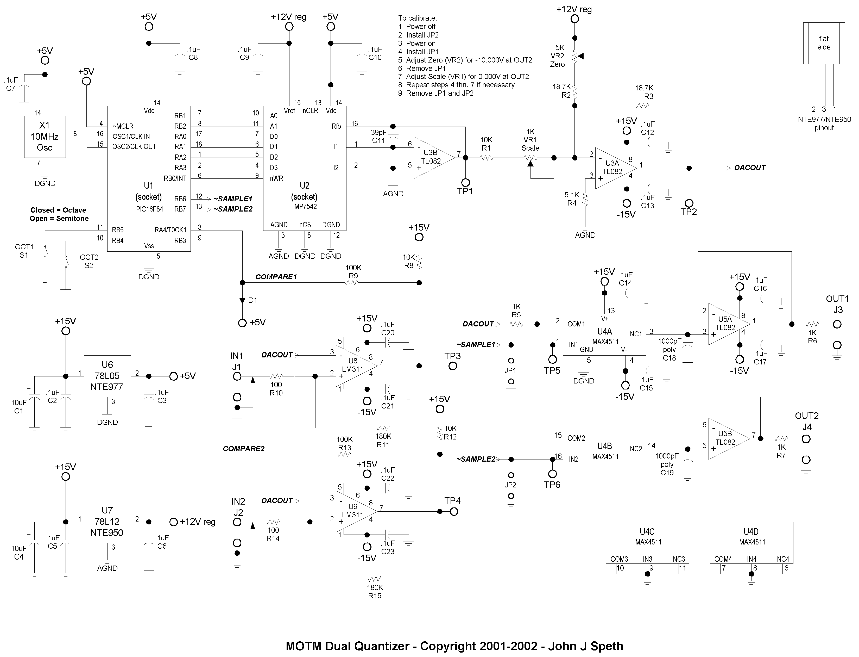
See the schematic and source code to follow the
design discussion. The circuit engine is a Microchip PIC16F84 microcontroller
(U1) clocked at 10MHz and an MP7542 12 bit DAC (U2). Op amp U3B converts the
current output of the DAC to a voltage output. Op amp U3A allows the trimming
of the zero voltage point and control voltage scale. The components used around
U3A were selected to achieve standard 1V/octave CV scaling. Channel 1
sample/hold is built around U4A, C18, and U5A. Channel 2 sample/hold is built
around U4B, C19, and U5B. Resistor R5 provides some slew limiting to keep down
noise. Channel 1 comparator is U8. Channel 2 comparator is U9. The 100W and 180KW resistors around the comparators provide about 8mv of
hystersis to reduce comparator chatter due to noise. The PIC and DAC are
powered by 5V. This voltage is supplied by U6. The DAC and zero/scaling
circuits require a clean 12V reference. This voltage is supplied by U7. Diode
D1 limits the maximum voltage at the PIC input RA4 to 5V. The internal
protection diode limits the maximum voltage at the PIC input RB3 to 5V.
Resistors R9 and R13 limit the current through internal and external limiting
diodes. Resistors R8 and R12 provide pull-up voltage to the open collector
outputs of the comparators.
The design is a two channel design in which
both channels CVs are quantized repeatedly and in order. A complete dual
channel quantization cycle begins with the PIC executing an 8 bit binary search
cycle to find the digital value of the control voltage, CV1, at the channel 1
comparator. This is essentially a digital to analog conversion process. The
channel 1 sample/hold is set to hold during the search cycle. When the search
cycle is complete, the channel 1 sample/hold is set to sample the DAC output
for a brief time to allow the hold capacitor to charge. After the sample time,
the PIC executes a quantization cycle on channel 2 similar to that of channel
1.
A 12 bit DAC was chosen to achieve the
accuracy needed for VCO control voltages. Only the 8 most significant bits are
used. Doing this, 12 bit accuracy is achieved in an 8 bit application. The
MP7542 was selected because I have many on hand. Any comparable 12 bit (or
better) DAC can be used with the appropriate software changes.
The design also uses an octave switch to use
octave (MOD12) quantization for control voltages. Closing the octave switch for
a given channel selects octave quantization otherwise semitone quantization is
used. This is a simple math function performed in software. This would suggest
that any quantization scales could be implemented with the appropriate software
changes. This is exactly what the Doepfer
A-156 Dual Quantizer does.
The PIC is clocked at the maximum rate of 10MHz
for the part I used. It may be clocked at lower frequencies but software
changes may be needed so as not to adversely affect the conversion interval per
channel. The DAC is loaded in about 6ms at 10MHz. The DAC
requires a 40ms settling period after loading the output register.
This time is consumed in the PIC software in a timed loop that does nothing.
The sample time is set to 1ms. This time is also consumed in the PIC software
in a timed loop that does nothing. The sample time consumes most of the conversion
cycle time.
Construction:
There were no unusual construction
circumstances. As usual, digital and analog grounds should be kept separate.
Digital circuitry should be located as far from analog circuitry as possible.
Sample/hold layout should be kept as tight as possible. All IC power pins
should be bypassed by .1m F capacitors.
All ICs used are DIP packaged with the
exception of the voltage regulators. The voltage regulators are packaged in the
TO-92 low power type packages. The PIC can be reprogrammed and, therefore, is
socketed using a high quality 18 pin DIP socket with gold plated contacts. The
DAC is socketed in case I want to hand select the DAC for accuracy. All other
components are soldered directly to the board. All resistors are 1/8W 1% metal
film. All 1% resistors were chosen to make parts ordering simpler. Resistors
R1, R2, and R3 are required to be 1% tolerance. All other resistors may be 5%
or 10% parts. Bypass capacitors are .1m F ceramic disc. The
sample/hold capacitors are 1000pF polystyrene which is critical for droop free
and accurate output. Potentiometers VR1 and VR2 are linear taper trimmers
mounted on the board. Octave switches S1 and S2 are mounted on the panel. Jacks
J1 through J4 are also mounted on the panel.
Calibration:
The quantizer must be calibrated to the
proper zero voltage and scale. Calibration only happens at power up. If any
jumpers are installed at power up, the quantizer goes into a calibration mode
in which one of three selected voltages is output to one or both of the CV
outputs. If, at any time, both jumpers are removed, the quantizer will go into
normal usage mode. CAUTION: INSTALLING A CALIBRATION JUMPER WHEN THE
QUANTIZER IS IN
The following table shows the output voltages
for the installation of the calibration jumpers:
|
JP1 |
JP2 |
Voltage |
Output |
|
In |
In |
-10.000V |
OUT1 and OUT2 |
|
Out |
In |
0.000V |
OUT2 |
|
In |
Out |
+10.000V |
OUT1 |
Here is the calibration procedure:
The zero voltage is defined as –10.000V out
when the input is at –10.000V. The output voltages should be calibrated to the
target voltages as closely as possible for accuracy. I believe that an average
person can discern pitch errors of 10 cents or more (100 cents in a semitone).
This translates to a calibration voltage accuracy of ± 4.2mV so your voltmeter will need to be at least this accurate. Some
people with better pitch hearing might require more accurate calibrations.
Software:
The PIC must be programmed before use. Click here for the hex code. The hex code may be programmed into
the PIC using any appropriate PIC programmer.
The hex code was built using the CC5X
C Compiler from B Knudsen Data. The
free edition of CC5X is perfectly suitable for compiling the source code. Click
here for the complete archive of the source code. The
source code is written entirely in C.
Suggestions for Future Designs:
The quantizer was built mostly from parts I
had on hand. This is how I chose the MP7542 DAC. I believe a better choice
would be the MAX551 from Maxim/Dallas. This part is essentially an MP7542 with
a serial data interface. It has better performance specs too. The serial
interface frees up microcontroller pins for other uses and makes construction
cleaner due to the fewer number of data interface lines between the PIC and the
DAC. Using the MAX551 will free up more pins for additional channels at the
expense of conversion time.
Additional quantization scales may be
implemented in software. The possibilities are potentially limitless.
The Doepfer
A-156 Dual Quantizer extends its’
usefulness by including a sample trigger input. I believe that when the jack
has a plug inserted, a conversion cycle is initiated by the edge of a digital
signal. I considered this feature on my quantizer but decided that this feature
is more appropriate for an outboard sample/hold. However, it is possible with
the appropriate simple hardware and software changes.
The PIC16F84 is an old die-hard chip for
flash programmable microcontrollers. Microchip has come out with many
alternative flash programmable microcontrollers in recent years. Any of the
PIC16F87X microcontrollers would give additional pins and higher possible clock
speeds that would enable feature rich designs based on my design presented
here. The feature set relies heavily on microcontroller software whereas the
hardware could be simple and static.
Pictures:
I’m sorry there are no pictures because I
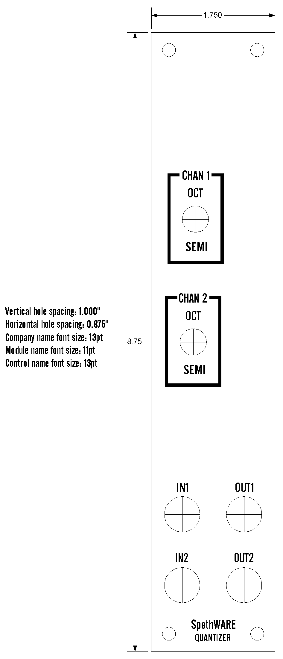
don’t have a digital camera. If I can borrow one, I will add pictures. Click here for a diagram of my front panel.